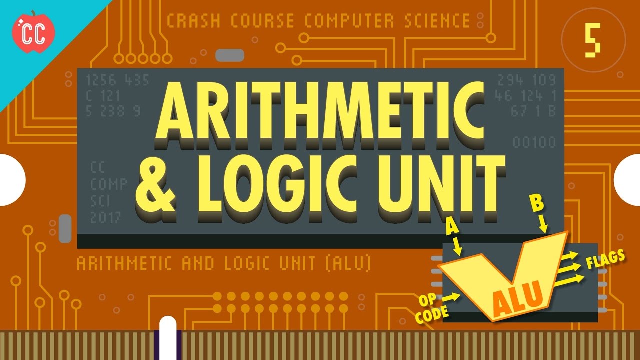
Sumador Rápido Simple y Lineal
En una serie de artículos y conferencias, he propuesto una arquitectura de "Sumador Rápido Simple y Lineal" para Unidades Lógicas Aritméticas (ALU, por sus siglas en inglés). El cuello de botella de Von Neumann, responsable en gran parte de la mayoría del retraso y el consumo de energía de un procesador, es evitado utilizando una arquitectura de Computación en Memoria (Compute-In-Memory). Este avance permite un procesamiento más rápido y eficiente en términos de energía, lo cual es crucial para el entrenamiento de redes neuronales e inteligencia artificial (IA), criptografía, modelado científico, investigación matemática, procesamiento digital de imágenes y otras aplicaciones intensivas que requieren ASICs, GPUs y TPUs de alto rendimiento.
Los sumadores rápidos tradicionales aumentan su complejidad y área proporcionalmente al cuadrado del número de bits. Sin embargo, el sumador propuesto tiene una complejidad de circuito constante, una profundidad de compuerta reducida y es escalable linealmente. Además de ofrecer una mejor eficiencia en tiempo y energía, el diseño, la producción y los costos de material también son menores. Este Sumador Rápido Simple y Lineal ofrece una ventaja aún mayor con respecto a otras arquitecturas, ya que permite implementar una arquitectura de Computación-En-Memoria para sumar múltiples entradas y multiplicar dos entradas. De las características más importantes de este circuito es que se puede escalar para lograr Multiplicación Rápida de Matrices In-Situ (Computación-En-Memoria).
La importancia de la Multiplicación de Matrices
La multiplicación de matrices es una operación fundamental en matemáticas, ciencias de la computación e ingeniería, que permite modelar y calcular relaciones complejas entre conjuntos de datos. Su eficiencia impacta directamente el desempeño de numerosas aplicaciones de vanguardia, entre ellas:
-
Inteligencia Artificial (IA) y Aprendizaje Automático (ML)
La multiplicación de matrices impulsa operaciones esenciales en redes neuronales, como la aplicación de pesos a entradas durante la propagación hacia adelante y hacia atrás. Afecta directamente la velocidad de entrenamiento y la escalabilidad de los modelos de IA, fundamentales para aplicaciones como procesamiento de lenguaje natural, visión por computadora y sistemas de recomendación. -
Gráficos Computacionales y Videojuegos
Transformaciones como rotación, escalado y traslación en gráficos 3D dependen de operaciones matriciales. La multiplicación de matrices permite renderizar en tiempo real para videojuegos, simulaciones y entornos de realidad virtual o aumentada. -
Criptografía y Seguridad
La multiplicación de matrices es fundamental para muchos algoritmos criptográficos utilizados en el intercambio seguro de claves, el cifrado y el descifrado. Acelerar estas operaciones mejora la eficiencia en la protección de datos sensibles, especialmente en aplicaciones en tiempo real. -
Computación Científica y Simulaciones
En campos como física, química y modelado meteorológico, las operaciones matriciales son cruciales para resolver simulaciones a gran escala y métodos numéricos. La multiplicación de matrices más rápida permite procesar modelos más complejos y precisos en menos tiempo. -
Análisis de Datos y Big Data
Técnicas como el análisis de componentes principales (PCA) y los modelos de aprendizaje automático utilizan la multiplicación de matrices para analizar correlaciones y patrones en conjuntos de datos masivos, generando información clave en sectores como finanzas, salud y marketing. -
Procesamiento de Señales
El procesamiento de señales digitales para datos de audio, imagen y video depende de la multiplicación de matrices para tareas como filtrado, transformaciones y compresión. Esta operación es integral para tecnologías como codificación MP3, compresión de video e imágenes médicas. -
Problemas de Optimización
Desde logística hasta robótica, muchas técnicas de optimización involucran resolver ecuaciones que dependen de operaciones matriciales. Una multiplicación de matrices rápida y eficiente acelera la toma de decisiones y la resolución de problemas en sistemas en tiempo real.
El costo computacional de la multiplicación de matrices aumenta rápidamente con el tamaño de las matrices. A medida que crece la demanda de potencia computacional, especialmente en campos como la IA, Big Data y la criptografía, los avances en hardware para la multiplicación de matrices serán esenciales para impulsar la innovación y abordar los desafíos futuros. Innovaciones como la Unidad Aritmética Rápida (FAU, por sus siglas en inglés), que incorpora multiplicación de matrices optimizada a nivel de hardware, son críticas.
Arquitectura In-Situ: Nuevas Fronteras para la Computación
La arquitectura tradicional de Von Neumann separa la memoria del procesamiento, lo que requiere mover datos entre estos componentes. Esto crea un cuello de botella significativo, especialmente en tareas con cargas masivas de operaciones como la multiplicación de matrices. La arquitectura de Computación en Memoria (CIM) elimina este cuello de botella al realizar cálculos directamente dentro de la memoria, ofreciendo varios beneficios transformadores:
-
Reducción de la Latencia: Al minimizar la transferencia de datos entre la memoria y el procesador, la CIM acelera significativamente las operaciones matriciales.
-
Eficiencia Energética: Los cálculos realizados dentro de la memoria reducen el consumo de energía, haciéndolo ideal para aplicaciones que requieren un rendimiento sostenido, como centros de datos y entrenamiento de IA.
-
Escalabilidad: La arquitectura admite el procesamiento paralelo de operaciones matriciales, crucial para tareas de computación de alto rendimiento.
-
Diseño Compacto: La CIM reduce el tamaño del hardware, permitiendo su integración en dispositivos más pequeños, desde móviles hasta nodos de computación en el borde.
Cuando se combina con hardware optimizado como la Unidad Aritmética Rápida (FAU), la arquitectura de computación en memoria amplifica el impacto de la multiplicación de matrices al proporcionar una velocidad y eficiencia computacional inigualables. Esta sinergia es particularmente vital para satisfacer las crecientes demandas de la IA, Big Data y sistemas en tiempo real.
-
Artículos
-
J. P. Ramírez, "Simple and Linear Fast Adder of Multiple Inputs and Its Implementation in a Compute-In-Memory Architecture," 2024 International Conference on Artificial Intelligence, Computer, Data Sciences and Applications (ACDSA), Victoria, Seychelles, 2024, pp. 1-11. (Archivo PDF).
-
On a Simple and Linear Fast Adder and Its Implementation for In-Memory Matrix Multiplication. Preprint.
-
-
Conferencias