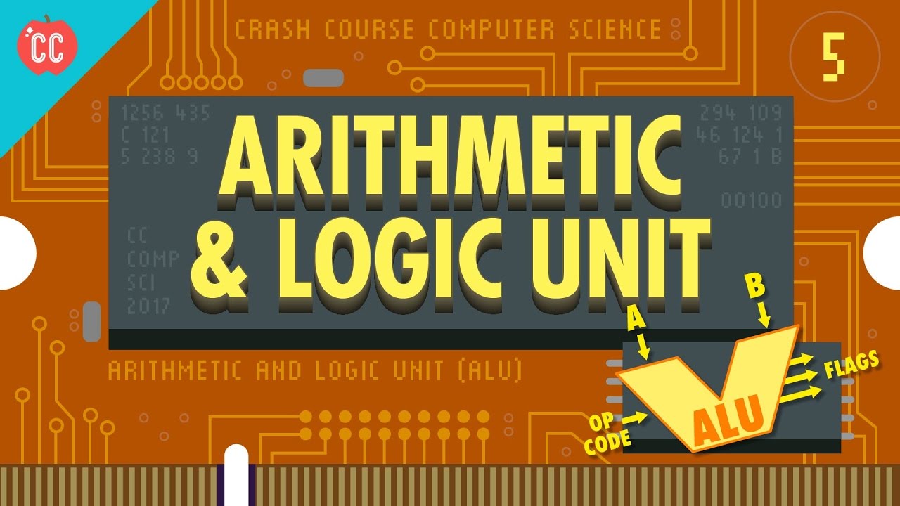
Simple and Linear Fast Adder
Although processors may seem fast and efficient, processing power is still insufficient. In a series of peer reviewed articles and conferences, I have proposed a “Simple and Linear Fast Adder” architecture for Arithmetic Logic Units. The Von Neumann bottleneck, which is responsible in large part for a processor's time delay and energy consumption, is bypassed with this design that seamlessly implements a Compute-In-Memory architecture without having to invest heavily in R+D for new memory and transistor types (SRAM/ReRAM/FeRam, etc.). This breakthrough enables faster, energy-efficient processors crucial for AI and ML, and other operation-intensive applications requiring high performance ASICs, GPUs and TPUs.
Other fast adders increase their complexity and area in proportion to the square of the number of bits. Our adder has constant circuit complexity, small gate depth, and it is linearly scalable. On top of better time and energy efficiency, reduced design, production and material costs, this Simple and Linear Fast Adder offers even greater advantage with respect to other architectures because a Compute-In-Memory architecture where addition of multiple inputs can be implemented. This circuit is also scalable to achieve fast In-Memory Matrix Multiplication.
This transformative IP represents a huge opportunity for AI hardware, cryptography, and edge computing innovations. The SLFA's in-memory computation capabilities are ideally suited for accelerating matrix operations in AI/ML processors, cryptography, and powering next-generation IoT devices. With its mathematically-proven efficiency and direct applications across trillion-dollar industries, this patent offers a decisive competitive advantage in the race toward post-Von Neumann computing architectures. The technology's CIM design makes it particularly valuable for neuromorphic systems and analog computing applications, while its foundational IP position creates opportunities for broad portfolio expansion.
The Significance of Matrix Multiplication in Modern Technology
Matrix multiplication is a cornerstone operation in mathematics, computer science, and engineering, enabling the modeling and computation of complex relationships between datasets. Its efficiency directly impacts the performance of numerous cutting-edge applications, including:
-
Artificial Intelligence (AI) and Machine Learning (ML)
Matrix multiplication powers the core operations of neural networks, such as applying weights to inputs during forward and backward propagation. It directly affects the training speed and scalability of AI models, which are foundational in applications like natural language processing, computer vision, and recommendation systems. -
Computer Graphics and Gaming
Transformations like rotation, scaling, and translation in 3D graphics rely on matrix operations. Matrix multiplication enables real-time rendering for gaming, simulations, and virtual or augmented reality environments. -
Cryptography and Security
Matrix multiplication is fundamental to many cryptographic algorithms used for secure key exchange, encryption, and decryption. Speeding up these operations improves the efficiency of securing sensitive data, especially in real-time applications. -
Scientific Computing and Simulations
In fields like physics, chemistry, and weather modelling, matrix operations are crucial for solving large-scale simulations and numerical methods. Faster matrix multiplication enables higher accuracy and more complex models to be processed in less time. -
Data Analysis and Big Data
Techniques like principal component analysis (PCA) and machine learning models leverage matrix multiplication to analyze correlations and patterns in massive datasets, driving insights in industries such as finance, healthcare, and marketing. -
Signal Processing
Digital signal processing for audio, image, and video data relies on matrix multiplication for tasks like filtering, transformations, and compression. This operation is integral to technologies like MP3 encoding, video compression, and medical imaging. -
Optimization Problems
From logistics to robotics, many optimization techniques involve solving equations that rely on matrix operations. Fast and efficient matrix multiplication accelerates decision-making and problem-solving in real-time systems.
The computational cost of matrix multiplication increases rapidly with matrix size. As demand for computational power continues to grow, especially in fields like AI, big data, and cryptography, advancements in matrix multiplication hardware will be essential to driving innovation and meeting future challenges. Innovations like the Fast Arithmetic Unit (FAU), which incorporates In-Memory matrix multiplication, are critical.
Compute-In-Memory Architecture: Unlocking New Possibilities
The traditional Von Neumann architecture separates memory and computation, requiring data to move back and forth between these components. This creates a significant bottleneck, especially for computationally intensive tasks like matrix multiplication. Compute-In-Memory (CIM) architecture eliminates this bottleneck by performing computations directly within memory, offering several transformative benefits:
-
Reduced Latency: By minimizing data transfer between memory and the processor, CIM significantly accelerates matrix operations.
-
Energy Efficiency: Performing In-Memory calculations reduces power consumption, making it ideal for applications requiring sustained performance, such as data centers and AI training.
-
Scalability: The architecture supports parallel processing of matrix operations, crucial for high-performance computing tasks.
-
Compact Design: CIM reduces the hardware footprint, enabling its integration into smaller devices, from mobile devices to edge computing nodes.
When combined with optimized hardware like the Fast Arithmetic Unit (FAU), the compute-in-memory architecture amplifies the impact of matrix multiplication by delivering unmatched computational speed and efficiency. This synergy is particularly vital in meeting the growing demands of AI, big data, and real-time systems.
-
Articles
-
J. P. Ramírez, "Simple and Linear Fast Adder of Multiple Inputs and Its Implementation in a Compute-In-Memory Architecture," 2024 International Conference on Artificial Intelligence, Computer, Data Sciences and Applications (ACDSA), Victoria, Seychelles, 2024, pp. 1-11. (Click here for PDF).
-
J. P. Ramírez, "On a Simple and Linear Fast Adder and Its Implementation for In-Memory Matrix Multiplication" (Preprint).
-
-
Conferences
-
“Simple and Linear Fast Adder based on a Simple Representation of Natural and Real Numbers”. Computer Science Special Session, 55 Mexican Congress of Mathematics, Guadalajara, Jalisco, 2022. (Click here for VIDEO)
-
"Simple and Linear Fast Adder of Multiple Inputs and It's Implementation for a Compute-In-Memory Architecture”. International Conference on Artificial Intelligence, Computer, Data Sciences and Applications, 1-2 February 2024, Victoria-Seychelles. (Click here for PDF)
-